ECC Technical Details
- What is ECC memory?
- How does ECC work?
- What's new in DDR5 ECC RAM?
- Is ECC memory neccessary?
- What system requirements are needed to enable ECC protection?
- How do I know when ECC errors are detected?
- How does MemTest86 report ECC errors?
- How does Windows report ECC errors?
- How does Linux report ECC errors?
- What is ECC injection?
- How can I test my ECC error detection and correction mechanisms?
- Why are ECC errors not being reported on my AMD Ryzen system?
- Why am I consistently seeing Correctable ECC / EDAC errors on my system?
What is ECC memory?
Error correction code (ECC) is a mechanism used to detect and correct errors in memory data due to environmental interference and physical defects. ECC memory is used in high-reliability applications that cannot tolerate failure due to corrupted data such as medical equipment, aircraft control systems, or bank database servers.
Most memory errors are single (1-bit) errors caused by soft errors (eg. cosmic rays, alpha rays, electromagnetic interference) but some can be due to hardware faults (eg. row hammer fault). Soft errors are more prevalent for systems that operate at higher altitudes, such as commercial aircrafts. It is said that at an altitude of approximately 10km, bit error inducing cosmic rays are 300 times higher.
Such single bit errors can be corrected by ECC memory systems. Multi-bit errors, may also be detected and/or corrected, depending on the number of symbols in error.
Symptoms of memory errors include corruption of data, system crash, and/or security vulnerabilities giving unprivileged code access to the kernel. Memory errors are known to be one of the most common hardware causes of machine crashes in large scale data centers.
How does ECC work?
ECC is implemented by generating and storing an encrypted, parity-like code used to not only identify the bit in error but correct it as well. This implementation-dependent ECC code is generated and stored on writes, and verified on reads.
The most common implementations use Hamming codes for single-bit correction and double-bit detection (SECDED). Hamming codes define parity bits which cover a pre-defined set of data bits. Typically, an 8-bit hamming code is used to protect 64-bit data.
The ECC verification step, using a parity-check matrix, generates a value called a syndrome. If the syndrome is zero, no error occurred. Otherwise, it is used to index a lookup table called the syndrome table to identifying the bits in error (if correctable), or otherwise determine if the error is uncorrectable.
An example of a syndrome table for the Hamming (7,4) code (4 data bits dn, 3 parity-check bits pn) encoded as p1p2d1p3d2d3d4 is as follows:
| Syndrome | Error Vector |
| 000 | 0000000 |
| 100 | 1000000 |
| 010 | 0100000 |
| 110 | 0010000 |
| 001 | 0001000 |
| 101 | 0000100 |
| 011 | 0000010 |
| 111 | 0000001 |
For example, if the ECC verification step calculates the syndrome to be 111, the above syndrome table can be used to lookup the error vector to be 0000001.
The error vector identifies d4 as the bit in error for the 7-bit message.
The sequences for read and write accesses are summarized below.
Memory write sequence
- CPU sends write data to the memory controller (on the same chipset, for newer CPUs)
- Memory controller generates ECC code based on the write data
- Memory controller sends write data and ECC code across the memory channel
- Write data and ECC code are stored in the memory DRAM chips
Memory read sequence
- CPU issues read request to the memory controller (on the same chipset, for newer CPUs)
- Memory controller reads data and ECC code from the memory
- Memory controller generates ECC code based on read data
- Memory controller verifies generated and stored ECC match. If not, use ECC SECDED mechanism to correct single-bit errors and detect double-bit errors.
Full end-to-end ECC memory system involves the CPU, memory controller, and DRAM modules during memory access. Consequently, these components require additional circuitry to support ECC functionality. For example, ECC RAM contains an additional DRAM chip to store the ECC codes as shown in the following diagram.
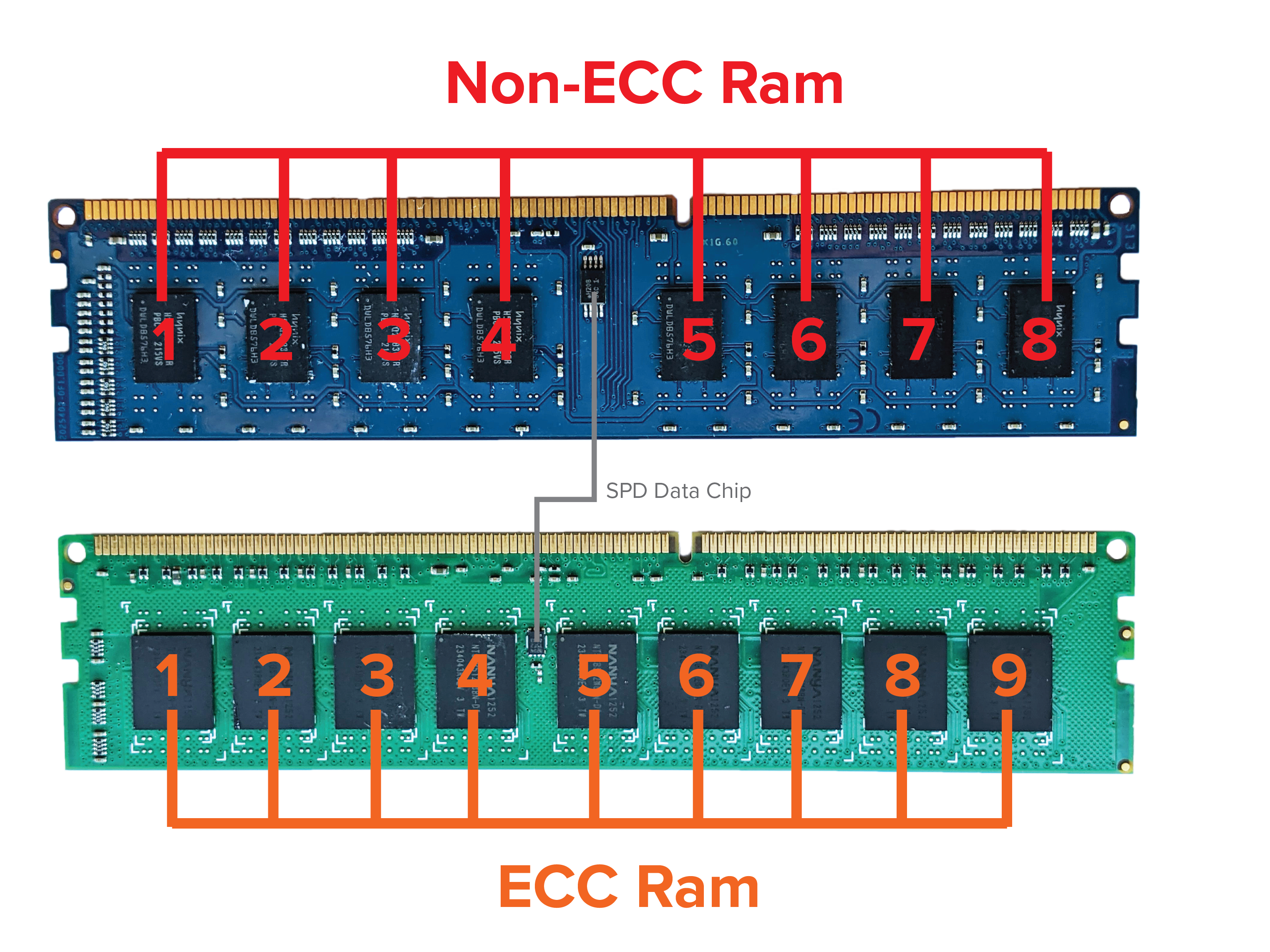
In addition, the memory bus not only includes the Data DQ lines (eg. DQ0-63) but also the ECC Check Bits CB lines (eg. CB0-7).
More often than not, ECC RAM is also Registered RAM which places a register between the memory controller and DRAM banks. This reduces the electrical load especially for systems that have a large amount of RAM installed, which is often the case for server-grade machines.
What are the different ECC schemes?
An ECC-enabled memory subsystem may use one or more of the following schemes:
- Side-band ECC (DDR4/DDR5)
- Inline ECC (LPDDR4/LPDDR5)
- On-die ECC (DDR5)
- Link ECC (LPDDR5)
Side-band ECC
Side-band ECC is the most typical scheme used in ECC memory systems today. Side-band ECC requires supporting hardware including ECC logic in the memory controller, extra bits in the memory bus and separate DRAM chips in the memory module to store the ECC code.
During write operations, the memory controller generates and transmits the ECC code alongside the write data as "side-band" without introducing extra command overhead.
On read operations, the stored ECC code accompanies the read data as "side-band" which is then verified, and if necessary, corrected by the memory controller.
Inline ECC
Inline ECC is used for LPDDR memory systems that have stricter hardware constraints. This effectively removes the requirements of extra bits in the memory bus and separate DRAM chips for the ECC code needed for Side-band ECC.
In contrast to Side-band ECC rather than bundling the data and ECC code in a single command, Inline ECC issues separate read/write commands for both the data and ECC code. In addition, the ECC code is stored in the same DRAM chips as the data. As a result, Inline ECC introduces extra command overhead during read/write operations.
On-die ECC
On-die ECC is a new scheme introduced for DDR5 memory which is completely self-contained in the DDR5 memory module.
On-die ECC, unlike the above schemes, does not provide end-to-end protection. The purpose of On-die ECC is to protect the integrity of data stored in the memory cells of DRAM arrays; it does not detect or prevent errors that occur during transmission between the memory controller and the memory module. All ECC detection and correction is performed internally within DRAM memory cells; it is completely invisible to the CPU and memory controller.
To provide full end-to-end protection, On-die ECC would need to be used in conjuction with Side-band ECC.
Link ECC
Link ECC is another new scheme introduced for LPDDR5 memory to augment end-to-end protection for systems with hardware constraints.
Link ECC, by itself, does not provide end-to-end protection; it provides protection for errors that occur during transmission on the channel between the memory controller and the DRAM.
On write operations, the memory controller generates and sends the ECC code along with the write data to the DRAM module. The DRAM module receives the write data, generates its own ECC code and verifies whether it matches with the ECC code sent by the memory controller. If necessary, single-bit errors are corrected accordingly.
In constrast to the other schemes, Link ECC does not detect or prevent errors while being stored in DRAM cells. To provide full end-to-end protection, Link ECC would need to be used in conjuction with Inline ECC to provide full end-to-end protection.
What's new in DDR5 ECC RAM?
Previous generation ECC memory systems Side-band and Inline ECC schemes which provides end-to-end detection and correction for errors during transmission and storage in DRAM cells
DDR5 RAM introduces two additional schemes, On-die ECC (or On-chip) and Link ECC, to compensate for higher bit error rates (BER) due to increased speed and density of DDR5 RAM.
On-die ECC detects and corrects errors in the DRAM cells that may occur during, for example, a DRAM row refresh. Due to increasing error rates as process technology reduces the size of memory cells, on-die ECC sustains the yield of "good" memory cells. On-die ECC is completely invisible to the system. Its implementation, encoding/decoding algorithms, and metadata are all fully contained within the DRAM device and provide no feedback about error detection and/or correction to the rest of the system
Similarily, Link-ECC detects and corrects transmission errors on the LPDDR5 link or channel. Compared to previous generations the likelihood of errors on the DQ line is much higher, due to significant changes in speed and power usage of LPDDR5 RAM. Link-ECC offers protection for speed and power improvements.
Is ECC memory neccessary?
In general, there is a trade-off between the higher cost of ECC hardware and slight decrease in performance versus greater system reliability and availability. Depending on the implementation, it is said that enabling ECC may consume additional power and lower memory performance by around 2–3 percent. For home or personal use, the consequence of memory errors may not be significant enough to justify the additional cost.
However, for highly-sensitive, industrial-grade systems, the additional hardware costs become neglible compared to the socio-economical consequences of memory failures. As a result, ECC memory should always be used in systems where memory failure has significant consequences (eg. medical equipment, aircraft control systems, bank payment system).
What system requirements are needed to enable ECC protection?
Due to additional circuitry required for ECC protection, specialized ECC hardware support is required by the CPU chipset, motherboard and DRAM module. This includes the following:
- Server-grade CPU chipset with ECC support (Intel Xeon, AMD Ryzen)
- Motherboard supporting ECC operation
- ECC RAM
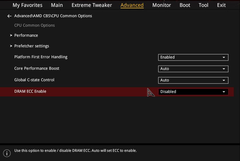
Do I need to change BIOS settings?
Most ECC-supported motherboards allow you to configure ECC settings from the BIOS setup. The specific option depends on the motherboard vendor or model such as the following:
- DRAM ECC Enable (American Megatrends, ASUS, ASRock, MSI)
- ECC Mode (ASUS)
An example of such ECC setting is shown in the following screenshot.
How do I know when ECC errors are detected?
The mechanism for how ECC errors are logged and reported to the end-user depends on the BIOS and operating system. In most cases, corrected ECC errors are written to system/event logs. Uncorrected ECC errors may result in kernel panic or blue screen.
How does MemTest86 report ECC errors?
MemTest86 directly polls ECC errors logged in the chipset/memory controller registers and displays it to the user on-screen. In addition, ECC errors are written to the log and report file.
During testing, MemTest86 may report ECC errors detected by the memory controller if ECC is supported and enabled. This is demonstrated in the following screenshot:
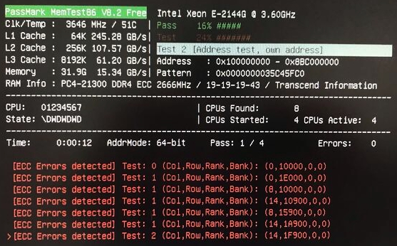
The degree of information available for the detected ECC error depends heavily on the CPU/memory controller chipset. This includes any of the following:
- Memory address
- DRAM address (column, row, rank, bank)
- Channel and DIMM slot number
The following examples illustrate possible outputs displayed on screen for detected ECC errors.
[ECC Error] Test: 1, Addr: 0x8F32540AC
The ECC error was detected in memory address 0x8F32540AC.
[ECC Error] Test: 1, (Ch,Sl,Rk,Bk,Rw,Cl): (1,0,2,0,17900,0)
The ECC error was detected in the DIMM module located in channel 1, slot 0 with the indicated rank address (0x2), and bank address (0x0), row address (0x17900), column address (0x0).
[ECC Error] Test: 1, Channel/Slot: 1/0
The ECC error was detected in the DIMM module located in channel 1, slot 0. No information regarding the memory address that triggered the ECC error is available.
*Note* The reported channel/slot of the ECC error is from the point of view of the memory controller and does not necessarily correspond to the expected physical slot on the motherboard. Although this is true for most motherboards, there are boards that do not map to the expected physical slot. One particular motherboard is the Supermicro H12SSL-NT which follows the physical slot mapping below:
| Reported channel | Motherboard slot |
| 0 | A1 |
| 1 | B1 |
| 2 | D1 |
| 3 | C1 |
| 4 | H1 |
| 5 | G1 |
| 6 | E1 |
| 7 | F1 |
Due to different memory controller architectures amongst different chipsets, there is no common ECC error framework; specific ECC polling code is required for each chipset. In particular, this would involve polling one or more of the following hardware registers:
- Machine Check Architecture (MCA) registers for x86-based systems
- Integrated Memory Controller (IMC) PCI registers
- Sideband registers for Intel SoC chipsets
- System Management Network (SMN) registers for AMD Ryzen chipsets
Machine Check Architecture (MCA) is an x86-specific mechanism for CPUs to report generic hardware errors to higher-level software (eg. operating system). This allows system software to handle hardware errors in a generic way, without needing to the internal details of chipset. It defines a common set of model-specific registers (MSRs) that deterine the system response when hardware errors are detected. In the case of ECC errors, an exception, Machine Check Exception (MCE), may be generated and the offending address, channel, and/or syndrome may be logged in the MSRs.
Some chipsets may also define a set of Integrated Memory Controller (IMC) PCI registers that record detected ECC errors such as the offending DRAM address (rank, bank, row, column), channel and/or syndrome. These registers are accessed through standard PCI mechanism. Unlike the Machine Check Architecture (MCA), the PCI registers are specific to each chipset and would required a separate chipset-specific implementation.
Some chipsets, such as Intel Atom SoCs, use an internal bus as an indirect method for accessing ECC registers. Such registers are called Sideband registers which adds an additional layer of complexity on top of the previously described PCI registers. Despite the extra layer, similar ECC error details are logged in these registers such as DRAM address (rank, bank, row, column), channel and/or syndrome.
For AMD Ryzen chipsets, an internal sideband bus called System Management Network (SMN) is used to access ECC registers. Similar to Sideband registers in Intel SoCs, SMN registers are an indirect way to access ECC error details logged in these registers such as DRAM address (rank, bank, row, column), channel and/or syndrome.
How does Windows report ECC errors?
ECC errors detected in Windows appear in the Event Log as Microsoft Windows Hardware Error Architecture (WHEA) Warning Event.
Log Name:      System
Source:        Microsoft-Windows-WHEA-Logger
Date:          1/1/2021 12:00:00 AM
Event ID:      19
Task Category: None
Level:         Warning
Keywords:
User:          LOCAL SERVICE
Computer:      WIN10
Description:
A corrected hardware error has occurred.

Reported by component: Processor Core
Error Source: Corrected Machine Check
Error Type: Cache Hierarchy Error
Processor APIC ID: 2
If ECC is enabled properly in the BIOS, end-users should be able to receive errors via WHEA without needing to configure anything in Windows.
How does Linux report ECC errors?
The Linux kernel supports reporting ECC errors for ECC memory via the EDAC (Error Detection And Correction) driver subsystem. Depending on the Linux distribution, ECC errors may be reported by the following:
mcelog- collects and decodes MCA error events on x86 (deprecated)edac-utils- fills DIMM labels data and summarizes memory errors (deprecated)rasdaemon- monitor ECC memory and report both correctable and uncorrectable memory errors on recent Linux kernels
Installing rasdaemon
rasdaemon can be installed for most Linux distributions using the respective package manager:
apt-get install rasdaemon # Debian/Ubuntu
Enabling rasdaemon service
The rasdaemon service can be started using the systemd service manager systemctl
                                        systemctl enable rasdaemon

                                        systemctl start rasdaemon
Querying ECC error count & summary
                                        # ras-mc-ctl --error-count

                                        Label                 CE      UE

                                        mc#0csrow#2channel#0  0   0

                                        mc#0csrow#2channel#1  0   0

                                        mc#0csrow#3channel#1  0   0

                                        mc#0csrow#3channel#0  0   0
                                        # ras-mc-ctl --summary

                                        Memory controller events summary:

                                        Corrected on DIMM Label(s): 'mc#0csrow#2channel#1' location: 0:2:1:-1 errors: 3

                                        Corrected on DIMM Label(s): 'mc#0csrow#3channel#0' location: 0:3:0:-1 errors: 3

                                        Fatal on DIMM Label(s): 'mc#0csrow#3channel#0' location: 0:3:0:-1 errors: 1
What is ECC injection?
ECC injection is a debugging feature introduced in the memory controller to artificially insert memory errors to verify proper system behaviour. This feature is meanted to be used by developers and system integrators, and not meant to be used in production by end-users.
Various ECC injection options are available depending on the vendor (eg. Intel, AMD) and chipset (eg. Xeon, Ryzen, Atom). These options include the following:
- Read and/or write data path
- Address range
- Per chunk count
- Single or Multi-bit errors
- Single-shot or continuous
Can I use MemTest86 inject ECC errors?
MemTest86 Pro Edition supports ECC injection if the CPU/memory controller chipset supports error injection and the feature is not locked by BIOS. See the current list of chipsets with ECC injection capability supported by MemTest86.
Once ECC injection is enabled in the main menu or configuration file, MemTest86 will attempt to inject single-bit ECC errors at the beginning of each test.
If ECC errors were successfully injected and detected by the system, the user shall see an [ECC Inject] message followed by an [ECC Errors Detected] message.
If [ECC Errors Detected] message does not appear, it is highly likely the ECC injection is locked or disabled by BIOS.
How do I know if my system supports ECC injection?
In general, ECC injection is not a feature that is normally accessible by end-users. Even if the chipset supports the ECC injection feature, details are often sparse and not described in publicly available datasheets. Consult the datasheet for your CPU/memory controller chipset to determine whether the ECC injection feature is available and fully specified.
In particular, some Intel chipsets (Broadwell, Xeon Scalable) use Intel Trusted Execution Technology (Intel TXT) to lock ECC injection. Intel TXT, using secure hardware modules, verifies the integrity of the BIOS, firmware, OS and hypervisor in order to guarantee a trusted operating environment. As a result, this requires preventing access to specific memory controller registers from being compromised, including ECC injection registers.
Some chipsets that support ECC injection have a locking mechanism that once enabled in the BIOS, effectively disables the ECC injection capability. For these cases, a BIOS option may be available to leave the feature unlocked. Otherwise, a custom BIOS is required for unlocking the feature.
How can I test my ECC error detection and correction mechanisms?
The PassMark ECC Tester is an DDR4 DIMM interposer, designed to inject single bit and double bit errors in real-time, to challenge and test the error detection and correction mechanism of machines that have CPU, motherboard and RAM sticks with ECC support.
It is connected to your system via USB, for tracking results, to change the ECC Testers setting, monitor voltages on the memory bus and allow MemTest86 and BurnInTest to control error injection.
Why are ECC errors not being reported on my AMD Ryzen system?
There is a possibility that a BIOS setting, Platform First Error Handling (PFEH), is preventing ECC errors from being reported to MemTest86.
An example of this setting is shown in the following screenshot.
If this setting is enabled, set to disabled and try running MemTest86 again.
Another explanation is the use of out-of-band (OOB) monitoring solutions such as Baseboard Management Controller (BMC) and Intelligent Platform Management Interface (IPMI), which is used in server platforms (eg. Supermicro servers)
Why am I consistently seeing Correctable ECC / EDAC errors on my system?
There is likely a bug in your EDAC/BIOS. Your ECC RAM is OK, but was not initialized properly by the BIOS on boot.
In order to initialize ECC, memory has to be written before it can be used. Usually this is done by BIOS, but with some motherboards this step is skipped if "Quick Boot" is enabled.
Possible Solution: If your system allows for it, try disabling Quick Boot in the BIOS, some error messages should disappear. The boot process may taker 30-60 seconds longer, but the EDAC error messages disappear due to the RAM check by the BIOS when booting.
BIOS known to experience this issue: KONTRON AMI BIOS


